1.In the Zener region the current ________ and the voltage across the diode ( ).
A:is almost constant; can increase a lot
B:can increase a lot; can increase a lot
C:is almost constant; is almost constant
D:can increase a lot; is almost constant
答案:can increase a lot; is almost constant
2.A ( ) is a combination of circuit elements, properly chosen, that best approximate the actual behavior of a semiconductor device under specific operating conditions.
A:monolithic IC
B:model
C:schematic
D:circuit
答案:model
3.What two parameters represent the FET transfer characteristic? ( )
A:drain-to-source voltage and drain current
B:drain-to-source voltage and gate-to-source voltage
C:gate current and drain current
D:gate-to-source voltage and drain current
答案:gate-to-source voltage and drain current
4.The input impedance of a voltage-shunt feedback amplifier ( ) the input impedance of its op-amp.
A:has no effect on
B:is increased when compared to
C:is decreased when compared to
D:is reduced by half when compared to
答案:is decreased when compared to
5.Which of the following FETs is the best choice when the gate-source voltage has both positive and negative swings? ( )
A:JFET
B:enhancement MOSFET
C:depletion MOSFET
D:CMOS
答案:depletion MOSFET
6.A class B push-pull amplifier ( ).
A:works only with digital and pulsed waveforms
B:conducts through 180° of the input waveform
C:conducts through less than 180° of the input waveform
D:conducts between 180° and 360° degrees of the input waveform, depending on the amount of dc bias
答案:conducts between 180° and 360° degrees of the input waveform, depending on the amount of dc bias
7.In the saturation region, the base-emitter junction ( ).
A:is forward-biased while the base-collector junction is reversed-biased
B:and the base-collector junctions are both forward-biased
C:is reversed-biased while the base-collector junction is forward-biased
D:and the base-collector junctions are both reverse-biased
答案:and the base-collector junctions are both forward-biased
8.The output impedance of a BJT is ( ).
A:capacitive
B:resistive
C:a combination of resistive, capacitive, and inductive
D:inductive
答案:resistive
9.( )biasing may be used with D-MOSFETs but not with JFETs.
A:Gate-drain
B:Gate-cutoff
C:Zero
D:Current-source
答案:Zero
10.The maximum current in a JFET is defined as IDSS and occurs when VGS is equal to ( ).
A:a voltage greater than the pinch-off voltage
B:pinch-off voltage
C:zero Volts
D:a small positive voltage
答案:zero Volts
11.Typical differential amplifier circuit changes from double-ended output to single-ended output, common-mode voltage gain ( ) .
A:increase
B:decrease
C:unable to determine
D:unchanged
A:saturation region B:active region C:cut-off region D:passive region 13.A relatively high input impedance, fast switching speeds, and low operating power describe the characteristics of the ( )family.
A:enhancement-type MOSFET B:CMOS FET C:BJT D:VMOS FET 14.Which of the following biasing combinations is not normally associated with one of the three transistor operating regions? ( )
A:E-B junction = reverse, C-B junction = forward B:E-B junction = reverse, C-B junction = reverse C:E-B junction = forward, C-B junction = reverse 15.The power-handling levels of a MOSFET ( ).
A:is usually about 100 W B:is usually less than 1 W C:is about 10 W D:is similar to that of a vacuum tube 16.In the integrated operational amplifier circuit, the ( ) coupling mode is adopted between the circuit of all levels.
A:resistance capacitance B:direct C:transformer D:photoelectricity 17.The fixed-bias technique requires ( ) power supplies.
A:2 B:4 C:1 D:3 18.If the resistor bypass capacitor in the source leg is removed, the voltage gain of the small signal FET amplifier ( ).
A:will increase B:will decrease C:will stay the same D:may increase in some cases and decrease in other cases 19.When comparing the common emitter and the common collector amplifiers, the input impedance of the common ________ is much larger and the output impedance of the common ________ is much smaller. ( )
A:emitter; collector B:collector; collector C:collector; emitter D:emitter; emitter 20.MOSFETs are also referred to as ( ).
A:DEFETs B:substrates C:SiO-FETs D:IGFETs 21.Which type of op-amp circuit has unity gain, no phase inversion, high input impedance, and low output impedance? ( )
A:summing amplifier B:subtractor C:voltage buffer D:differentiator 22.Depending on the configuration of the amplifier, the magnitude of the no-load current gain for a single BJT transistor amplifier typically ranges from ( ).
A:10 to about 10,000 B:one to about a thousand C:just a little less than 1 to a level that may exceed one hundred 23.For a two-port system, like a BJT amplifier, the no-load voltage gain ( ).
A:is always less than the loaded voltage gain B:can be less than or equal to the loaded voltage gain C:is always greater than the loaded voltage gain D:is always equal to the loaded voltage gain 24.Current-series feedback ( ) the input impedance of an op-amp.
A:reduces by half B:decreases C:has no effect on D:increases 25.The value of drain current is always ( ) the value of the short circuit drain current IDSS for a given JFET.
A:greater than B:equal to C:less than or equal to D:less than 26.The input impedance of a common-base BJT configuration is typically ( ).
A: between 100 kΩ and 10 MΩ B: between 100 Ω and 100 kΩ C: so large that the input current can be considered to be zero D: less than 50 Ω 27.A class D amplifier ( ).
A:conducts through less than 180° of the input waveform B:works only with digital and pulsed waveforms C:conducts through 180° of the input waveform D:conducts between 180° and 360° degrees of the input waveform, depending on the amount of dc bias 28.The diffusion capacitance of a diode is a shunt capacitance effect that occurs when the diode( ).
A:is forward biased B:is large C:is reverse biased D:is small 29.The simplest biasing arrangement for the n-channel JFET is ( ).
A:voltage-divider bias B:drain-feedback bias C:variable bias D:fixed bias 30.Generally, it is a good design practice for linear amplifiers to choose the operating point that is approximately ( ).
A:near the cut-off region B:in the center of the active region C:near the origin D:near the saturation region 31.Depending on the configuration of the amplifier, the magnitude of the no-load voltage gain for a single BJT transistor amplifier typically ranges from ( ).
A:10 to about 10,000 B:a hundred to about a million C:just a little less than 1 to a few hundred 32.The maximum possible efficiency of a class A amplifier is equal to ( ).
A:15 B:25% C:30% D:20% 33.In most cases, which two of the three BJT terminal currents are approximately equal in value?( )
A:collector current and base current B:collector current and emitter current C:All currents are approximately equal. D:emitter current and base current 34.Some of the modern ohmmeters have a diode test setting. If you do not have one of these ohmmeters then to test the diode you need to check its resistance in the forward and the reverse direction. These resistances should be ( ).
A:relatively low in the forward direction and relatively low in the reverse direction B:relatively low in the forward direction and relatively high in the reverse direction C:relatively high in the forward direction and relatively high in the reverse direction D:relatively high in the forward direction and relatively low in the reverse direction 35.In the design of an emitter-bias stabilized circuit engineering, judgment must be used because the ( ).
A:emitter resistor is usually unknown B:Not at all C:relative voltage levels have not been defined D:collector resistor is usually unknown 36.When a BJT is biased in the cut-off region, its base-emitter junction is ________-biased and its collector-base junction is ________-biased. ( )
A:forward; forward B:reverse; forward C:forward; reverse D:reverse; reverse 37.MOSFETs typically have an input impedance value that is ( ).
A:equal to the JFET B:higher than the JFET C:lower than the JFET D:randomly defined relative to the JFET 38.Class D amplifiers have a maximum theoretical efficiency of ( ).
A:78.5% B:over 90% C:25% D:50% 39.When a p-n junction's depletion layer is narrowed and the device acts as a nearly perfect conductor, it is ( ).
A:forward-biased B:reverse-biased C:unbiased 40.Enhancement-type MOSFETs operate in the ( ).
A:depletion mode and the enhancement mode B:depletion mode only C:enhancement mode only 41.The h-parameter model uses ( ) parameters to describe the equivalent circuit of the BJT transistor.
A:five B:four C:two D:three 42.Op-amp differentiator circuits differ from the integrators in that the differentiators ( ).
A:have a scale factor of -RC B:are not as useful C:have a resistor in the feedback loop 43.The advantage of negative feedback is ( ).
A:higher input impedance B:lower output impedance C:voltage gain that is more stable 44.Why is design for a specific bias point desirable for most amplifiers? ( )
A:It allows optimum dc operation of the circuit. B:It allows optimum ac operation of the circuit. C:To meet manufacturer suggested opening point. 45.The voltage gain of a FET amplifier is generally larger than that of a comparable BJT amplifier.( )
A:对 B:错 46.The input impedance of a FET amplifier tends to be much greater than a comparable BJT amplifier.( )
A:对 B:错 47.
A given BJT has an emitter current of 12 mA and a base current of 600 μA. What is the value of  ?( )
?( )
A:20 B:21 C:200 D:19 48.
Calculate the base current for this emitter-stabilized bias circuit.( )
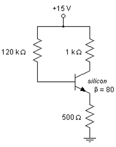
A:89.0 mA B:89.0 μA C:0.119 mA 49.
An E-MOSFET has values of  = 4 V and
  = 12 mA when
  = 10 V. The device is being used in a circuit that has a value of
  = 6 V. What is the value of
  for the circuit? ( )
A:1 mA B:1.33 m C:13.33 mA D:0 mA 50.
The current gain  of an FET amplifier is ( ).
A:undefined B:depends upon the value of for the device C:generally assumed to be zero D:less than or equal to 1 51.
The voltage gain for this circuit is give as ( ).
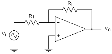
A: B: C: D: 52.
When the input voltage to this circuit is 0.25 V, the output voltage is ( ).
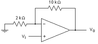
A:5.0 V B:1.5 V C:10.0 V D:3.0 V 53.
A constant-gain multiplier has three stages and a total gain of 22,200. For all three feedback resistors,  = 470 kΩ. Two of the
  resistors have a value of 33 kΩ. What is the value of the third
  , and what is the nature of its stage? ( )
A:4.6 kΩ, noninverting B:4.3 kΩ, inverting C:4.26 kΩ, ohms, inverting D:4.3 kΩ, ohms, noninverting 54.
Which of the following is true for this circuit?( )
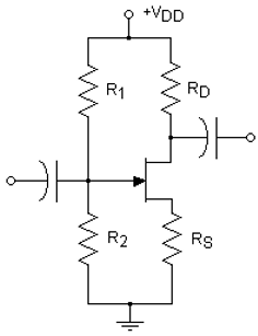
A: is equal to the voltage across B: is measured between the gate and common C: is measured between the gate and source terminals D: is always close to +0.7 V 55.
The base-10 logarithm of 1780.331 ( ).
A:3.2505 B:0.335 C:33.5 56.
Calculate the quiescent drain current for this self-bias depletion mode MOSFET transistor amplifier.( )
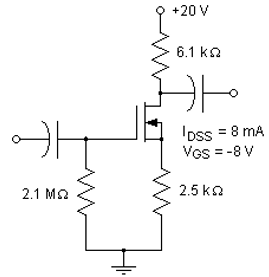
A: B: C: D: 57.
If this circuit is to have an inverting voltage gain of 1, the ratio of  :
:  should be ( ).
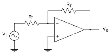
A:1: 2 B:2 : 1 C:Cannot be done in theory. It can be done in practice by making much larger than D:1 : 1 58.
This is a basic ( ) circuit.
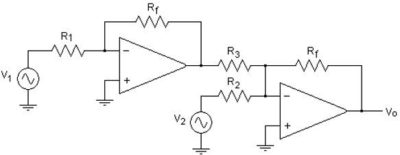
A:two-input multiplier B:integrator C:differentiator D:subtractor 59.
This is the symbol for a ( ).

A:ppn-type BJT B:pnp-type BJT C:pnn-type BJT D:npn-type BJT 60.
Which of the following expressions is true? ( )
A: B:where is constant C: D:where is constant

